
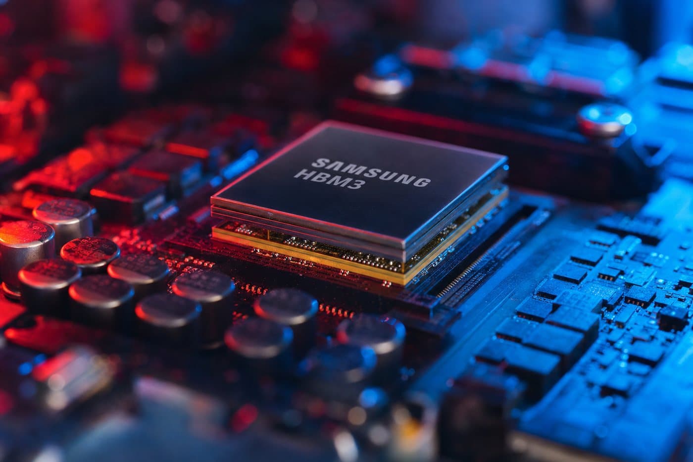
President Lee Jae Myung opened the first project of South Korea's industrial megaproject plan at Samsung's Onyang campus: a US$4.3 billion (6 trillion won) advanced-memory packaging fab, to be followed by about US$28.8 billion (40 trillion won) in equipment.
South Korea broke ground on Thursday, 12 November, on the first project of its industrial "megaproject" initiative, a high-bandwidth memory (HBM) packaging plant at Samsung Electronics' Onyang campus in Asan, South Chungcheong Province, The Korea Herald and Reuters, via CNA, report. President Lee Jae Myung attended with Samsung Electronics Chairman Lee Jae-yong, four months after the government unveiled the plan.
The president said Samsung's US$4.3 billion (6 trillion won) investment in the advanced packaging fab would be followed by about US$28.8 billion (40 trillion won) in phased investment in advanced equipment. Samsung said the new line, Onyang Line 5, has been brought forward by about a year and is due to start operating in June 2028; the three-storey plant will have about 31,000 square metres of cleanroom space and, according to The Korea Herald, will produce next-generation HBM4E chips as demand for AI memory strains supply.
The megaprojects, announced in late June, cover semiconductors, AI data centres and physical AI and aim to steer investment outside the Seoul metropolitan area. In July Samsung, SK Hynix and other large companies announced plans to invest about US$282 billion (392 trillion won) in the Chungcheong region. President Lee said local governments had cut permitting times to about a third of the usual, and that 112 companies in sectors including semiconductors and biotechnology are expected to invest a further US$17 billion (23.6 trillion won) in the region. Kim Young-jae, chairman of Samsung supplier Daeduck Electronics, said 194 Korean materials, parts and equipment companies plan to invest US$13 billion (18.1 trillion won) by 2030.