
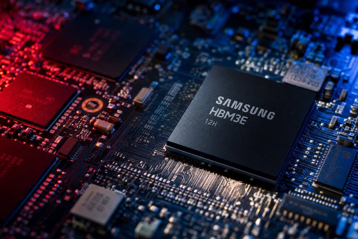
President Lee Jae Myung says the Asan chip packaging line will be followed by heavy spending on equipment as Korea chases AI memory demand.
Samsung Electronics' US$4.3 billion (6 trillion won) plant for packaging high-bandwidth memory chips in Asan, South Korea, will be followed by about US$28.8 billion (40 trillion won) of investment in advanced equipment, President Lee Jae Myung said at the groundbreaking on Thursday, 12 November, according to a Reuters report carried by CNA.
The ceremony covered part of the investment plans Samsung affiliates announced in July. Samsung said the new HBM line is due to begin operating in June 2028, a year ahead of the original schedule, as it tries to keep up with fast-growing demand for server memory used in artificial intelligence. The building will have three floors of clean rooms covering about 31,000 square metres.
High-bandwidth memory is stacked memory used alongside AI processors in data centres. South Korea's government has asked Samsung, SK Hynix and other companies to lead national "mega projects" in semiconductors, physical AI and AI data centres.